How to manufacture hardware.
as a start-up... in the US... (*mostly)...

This is a high-level overview of the process I went through to build my first hardware product in the US*. There are a lot of links to resources that could help you on a similar journey. This guide is by no means comprehensive, or likely even good advice. But it’s what I wish I knew at the beginning, and I’m hoping it will help people who are just getting started. I would love feedback, critiques, or additional pointers that may help others. The resources linked here are listed in a GitHub repo; pull requests or email feedback/pointers are very welcome.
Caveats:
- I’m a software guy. No Electrical Engineering (EE) or hardware experience prior to this. No industry or manufacturing knowledge. In essence, in this domain, I was (am?) a “non-technical founder”.
- I’ve learned enough to get my product built. I’m still swimming near the beach, but the hardware-manufacturing ocean is vast and deep. I am missing a LOT here, but will keep updating and adding to it.
- This is an effort to share knowledge so that others can move faster and build better. But treat this as more of a story than a manual.
Who is this for?
Other founders who are interested in making a physical product but have never done it. Software start-ups that are “hardware curious” or have a physical product on their roadmap. Hackers, tinkerers, and makers who maybe want to know what the next steps looks like.
Outline:
A word about hardware vs. software iteration cycles: “hardware is hard”. In software, even waterfally, bureaucratic, change-controlled dev-test-QA cycles are cheap and fast (by comparison). In hardware they cost real out-of-pocket money (physical components, circuit boards, fab & assembly, shipping, etc.) and take a long time (days or weeks, if not months). If you combine this expensive, slow cycle, with the need to learn from feedback and testing, and alter design frequently, you will get a very long and expensive time-to-market. This may not be the ideal model, but what I’ve settled on is three iteration loops, two of which potentially overlap. This article is structured along those lines:
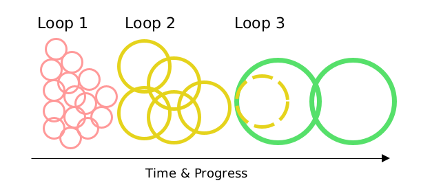
Loop 1: Lots of short cycles till you get to proof-of-concept (which is not an MVP).
1. Experimentation, learning, and tools
1. Experimentation, learning, and tools
Loop 2: medium cycles, but expensive and slower, till you get to prototype
2. Component Selection
3. PCB Design
4. Firmware Development
5. Case Design
2. Component Selection
3. PCB Design
4. Firmware Development
5. Case Design
Loop 3: most expensive, but fewest unknowns, ideally two or less of these cycles
6a. Design-for-Manufacturing
6b. Changes may require further “Loop 2” cycles..
6c. Production
6a. Design-for-Manufacturing
6b. Changes may require further “Loop 2” cycles..
6c. Production
1. Experimenting, learning, and design tools used:
Sketch out your idea on pen and paper, maybe use logical diagramming tools or even UI wireframe tools to mock-up how you want things to work. Tindie, Hackaday, Sparkfun, and Adafruit are great resources to find existing or similar projects, inspiration, or just to learn. You may find something close to what you are trying to build or at least components of it there.
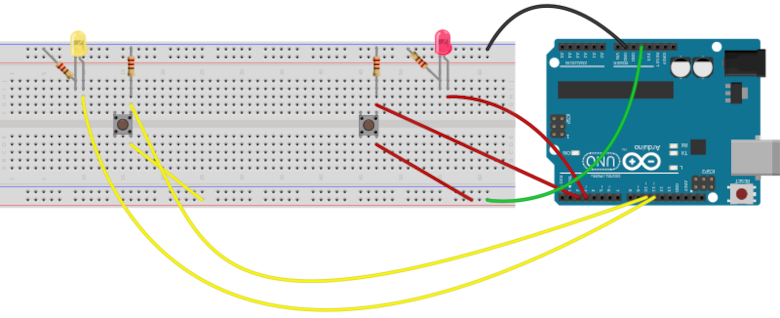
You may start with Raspberry Pi’s, Beagle Boards, and/or Arduino’s, and use Sparkfun or Adafruit breakout boards to hack together a proof-of-concept. KiCad is great open source software for laying out schematics and circuit board designs. Sparkfun is really a good learning resource for basic EE concepts. Similar to learning to code, you may find it easiest to start altering an existing project or connecting simple parts. Adafruit and Sparkfun are awesome at publishing their break-out board files. Breadboards and prototype boards will be your friends.
I highly recommend that you get as close as you can to a full working model at this stage. Forums are often your best sources of advice and finding out how others may have solved a similar problem. This is also a good time to learn the new debug and testing tooling you will need in the hardware world, such as how to use a multimeter if you don’t already know. This is also the stage you are going to want to learn about burning in bootloaders or firmware.
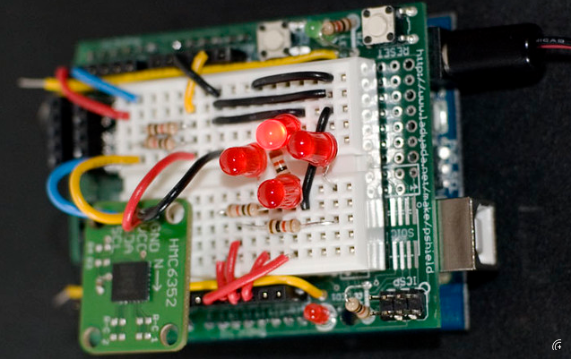 Photo: syvwlch
At the end of this experimental stage you should have your idea working in software, logical design sketched out, maybe usage mocked up, and ideally a bread board with the critical hardware components connected and working. Maybe even things glued together as a working proof-of-concept. This should give you a rough idea of what components (chips, etc.) you will need and maybe a sketch of your own Printed Circuit Board (PCB).
2. Component selection:
Once you have a proof-of-concept of what you want to build, the next step is Component Selection for your own PCB(s). My advice is to first build your own breakout boards of the major components in your design, using your intended chips. As you iterate through design and components selection having modular "building blocks" to connect can save you having to rebuild the whole PCB each cycle.
You likely won’t be able to find all the components you need manufactured in the US. You may, however, want to avoid China due to security risks or supply-chain disruption. Side note: there are some great entrepreneurs in China and a lot of innovation. The issue, however, is that they fall under the control of the CCP, which can put your product at risk for a variety of reasons.
One reasonable way to work through the component selection for your Bill of Materials (BoM) is to use Arrow’s “Country of Origin” designator. Sadly they do not expose that as a search or filter column selection in their normal online tool. Enterprise customers may have access to a different tool that allows that, but I never saw it. Unfortunately, I could not find Country of Origin listed anywhere on Mouser (my preferred shop) or Digikey. With some elbow grease you should be able to crawl through your first version of BoM on Arrow and ensure that all your components are sourced from the US or other reliable countries. Another side note: I spent a good amount of time trying to get the large chip manufacturers to give me lists of their products that were made in the US, with no success. Aside from being a pissant start-up and not worth talking to, I also think their sales staff have no visibility into the ever-changing supply chain inside their own companies.
3. PCB Design:
For early prototypes or breakout boards you can either figure out how to do surface mounting of components in-house or use a prototyping shop like RapidPCB. The RapidPCB guys are a few doors down from me in the same office park. I trust them completely and they have been super helpful. There are many similar shops all over the country but notable concentrations in Austin, the Bay Area, Chicago, Seattle, and Boston. Another possible path to find engineering consulting help, is on Tindie. Many sellers are open to custom work, and possibly built something similar or are using the same components as you.
For in-house builds, you can get PCBs done by OSHPark and surface-mount your components with a hot plate or small oven. This is an investment and a skill that needs developing, but it's worth it if you are bootstrapped or otherwise constrained. It also can speed up your iteration cycles, after the set-up and learning-curve time. The caveat with this is that it can be difficult to pin down what are manufacturing-flaws vs design-flaws, if your manufacturing skills are sketchy. Trust me, wasting hours (or days) on firmware and design changes, only to find out it was just a soldering or mounting flaw is not fun. Not that it’s ever happened to me.. multiple times..
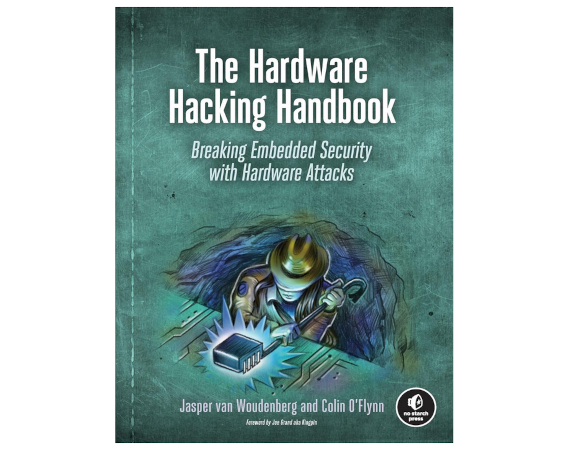
I highly recommend that you read “The Hardware Hacking Handbook” at this stage (if not sooner). Assurance, or reliability, is very likely important in your final product, even if it is not itself a security product. Further it helps with understanding a lot of the concepts involved at this stage. You will also want to follow the very cool PCB Design Checklist to make sure it's squared away.
4. Firmware (i.e. software by another name):
Part of designing and validating your circuit board is to ensure that it can run your software, reliably, at the speeds you need it to. Now that you have a first pass of your components and circuit board layout, you should build test firmware. The primary focus at this stage is to ensure that the manufacturing output is correct and supports your overall design. Another issue to consider, is the loading, and potential updating, of the firmware onto your production system. Who will load the production firmware during the manufacturing process and how? Some fabs offer a burn-in process as part of the PCB assembly, for example. The next consideration is once the product has shipped, who will apply any updates and how? Other considerations may be security of the production firmware.
 Image: MesserWoland
You may also want to do a “dev” build of your circuit board that makes it faster and easier to iterate during the software development cycle. For example you may not have a USB header port or OLED display connected directly to your MCU in the final product, but you may want to add one during development. This can make it easy to connect to your workstation for quicker firmware flash, test, and debug cycles. You may also want to add debug interfaces like a SWD header that may not be present in your production unit. Much of this you will have already tackled in the experiment/bread-board phase. Now the focus is to test your physical design, as well as the output of the manufacturing process.
One trick, that can speed up testing, is to build your own custom breakout board of your MCU, modeled off one that already has Arduino support (again, thanks to Sparkfun and Adafruit for their awesome open-source support). You then only need to modify the board variant definition files and you can quickly use Arduino bootloaders and libraries to test your design. The other path is to go all-in on the vendors IDE and build system. This is where you will likely need to end up for production. While ST has the most developer-friendly IDE and ecosystem, Microchip comes in a close second, with one shitty requirement of Windows for their IDE (warning: a LOT of hardware vendors only support Windows for some reason… blech!)
5. Case Design:
Now that you have worked through Component Selection and have a design for your circuit boards, you’ll want to spend a little effort on case design. Often you may need to adjust the circuit board or add mounting holes and such for optimal case design. What you produce here, very likely, won't be production-ready, but it will prepare you for the Design-for-Manufacturing process and get you in the ballpark. It will likely feedback into PCB design iterations and end up with cut-outs or holes. Thingiverse may be a good place for inspiration.
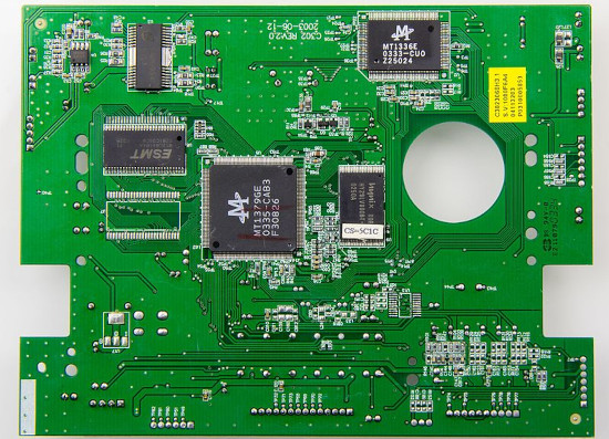 Photo: Raimond Spekking
You can export your KiCad PCB file into other tools to help design an STL file for your case. You can then upload your STL to Shapeways or CraftCloud to get it made using a variety materials. Note that in CraftCloud, you need to choose your actual printers: it’s just a marketplace. One printer that I’ve had great success with is JawsTech, out of Idaho. Unlike Craftcloud, Shapeways does everything in-house and their quality and expertise are solid, albeit more expensive and ships from EU.
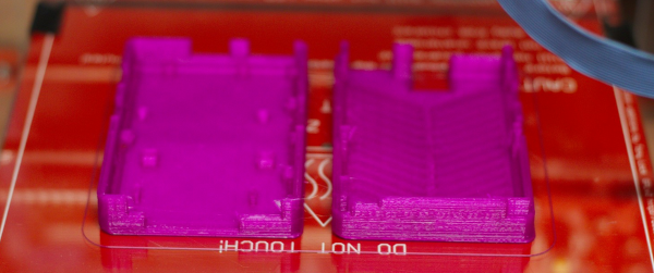 Photo: Dennis van Zuijlekom
You can also use OSHCut, out of Utah, for laser cutting sheet metal components. They also offer other services such as metal bending, from your uploaded 3D files. McMaster-Carr is a great resource for mounting hardware (and an amazingly well designed website). You may need cables or interconnects to other systems. Companies like Freedom Atlantic can help you there. They also have a broad range of expertise in real-world application (and abuse) of your product so may be able to offer a good bit of guidance.
6. Design-For-Manufacturing and Production:
You will likely need to test, refine, and iterate on the above steps at least a few times. Or if you are “learning as you go” like me, dozens of times. But when you finally have a decent BoM, PCB, and case design, and you need to start producing more than a handful, you’ll have to start thinking about “design-for-manufacturing” and finding partners for that. Threshold Strategic Consulting, with facilities in Cleveland, can assist in that process and can guide you through decision criteria on, for example, injection molding vs. additive manufacturing, among other things. We are using MacroFab, out of Houston, for large-scale PCB manufacturing. I highly recommend both of them. They are responsive and helpful, ITAR compliant (if needed), and not over-priced. They offer an array of services that may help you in production.
Finally, your product could require an assembly and warehousing stage. We are doing this in-house and the only advice I can offer about this is it takes time to work out. There are service providers out there that can manage this for you, but in my limited research, their minimum volumes were too high for early-stage or bootstrapped production, or too expensive, or not secure enough for our needs. If you have security requirements, then keeping this in-house is going to be FAR more cost-effective, for comparable levels of trust/risk.
ASICs… wwuUUhhhh?!?!:
Something that I want to mention, that I have not used yet but is on the horizon, is Tiny Tapeout and the ecosystem around that project. FPGA’s are they obvious solution for many problems, but I’m excited about the design efficiency improvements that are coming to the ASIC world. It is worth keeping an eye on it, and it may not be the insane, out-of-reach option in the future that it has been.
Resources List:
All of the resources in this piece are posted on our site and on GitHub. Sometime down the road I will need to develop this same partner list in the EU, as we start manufacturing there for customers in that region. As I mentioned, I’m almost still in the kiddie-pool end of the manufacturing ocean. I have learned just enough to get my product (nearly) out the door. If you know of resources that will help others create products, please reach out (pull requests, email, whatever).